
ACE800333 is an optimized product from Accelerated Computing Engineering that performs a concatenated multiplication of $3 \times 3$ matrices ($D = A \times B \times C$).
Intended for algorithmic workloads requiring FP32 $3 \times 3$ matrix concatenation, the ACE800333 is developed following the ACE standard development methodology that achieves low resource utilization while maintaining IEEE-754 FP32 accuracy. (For Intel/Altera Cyclone V deployments, see the pin-compatible sister core ACE80A333.)
xazu1eg-sbva484-1-i FPGA (the smallest member of the AMD UltraScale+ family)The core implements a concatenated matrix multiplication engine designed for high-density arithmetic throughput. The primary operation is defined by the following transformation:
$$D = (A \times B) \times C$$
where $A, B, C \in \mathbb{R}^{3 \times 3}$ are real square matrices. To support multi-stage verification and nested algorithms, the core also provides direct memory-mapped access to the intermediate product:
$$X = A \times B, \qquad D = X \times C$$
with each element evaluated via IEEE-754 left-associative dot products:
$$X_{i,j} = \sum_{k=0}^{2} A_{i,k} B_{k,j}, \qquad D_{i,j} = \sum_{k=0}^{2} X_{i,k} C_{k,j}$$
All elements—including input operands, intermediate products, and final results—are defined and operated in the IEEE-754 Single-Precision Floating-Point (FP32) arithmetic format:
Post-implementation utilization on an entry-level AMD Zynq UltraScale+ (xazu1eg-sbva484-1-i):
The core runs on two different clocks:
CLK_FAST with a maximum frequency of 200 MHzCLK_SLOW that shall run at 50 MHz (phase aligned with CLK_FAST)
CLK_SLOW is used for the ACE800333 initialization, while CLK_FAST is used for all the runtime operations. In the verification project, the timing was closed with a robust 2.517 ns timing margin (WNS) and with 0 timing violations.
The Concatenated $3 \times 3$ Matrix Multiplier core is packaged as an AMD IP core. Figure 1 illustrates the verification configuration.
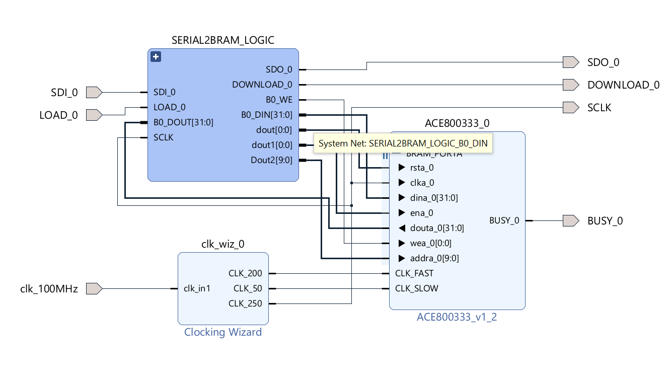
The core is fully controlled through read/write operations on a BRAM (optionally accessible via an AXI BRAM_CONTROLLER). The instantiated BRAM is 1 True Dual Port with port A available to the user and port B managed by the internal Math Engine. The BRAM has a width of 32 bits and a depth of 1024 locations. The core uses the first 53 locations (0–52), with the remaining ones completely available for the user via port A.
| BRAM | ADDRESS | VARIABLE | DIR | FORMAT | DESCRIPTION |
|---|---|---|---|---|---|
| BRAM_0 | 0 | START_CMD | IN-OUT | BINARY | Set to 0x1 by the user to start the computation. Set to 0x0 by the math engine at the end of computation. |
| BRAM_0 | 1 | DNA1 | OUT | BINARY | DNA (63 downto 32). The core uses 64 bits (zero-padded MSB if shorter) for compatibility across FPGA generations. |
| BRAM_0 | 2 | DNA2 | OUT | BINARY | DNA (31 downto 0). |
| BRAM_0 | 3 | USER_KEY1 | IN | BINARY | USER_KEY (63 downto 32) |
| BRAM_0 | 4 | USER_KEY2 | IN | BINARY | USER_KEY (31 downto 0) |
| BRAM_0 | 5 .. 13 | a00 .. a22 | IN | FLOAT 32 | Input Matrix $A$ elements, row-major ordering ($a_{00}, a_{01}, \dots, a_{22}$) |
| BRAM_0 | 14 | RESERVED | N/A | — | Memory alignment boundary |
| BRAM_0 | 15 .. 23 | x00 .. x22 | OUT | FLOAT 32 | Intermediate Matrix $X = A \times B$ elements, row-major ordering ($x_{00}, x_{01}, \dots, x_{22}$) |
| BRAM_0 | 24 .. 32 | d00 .. d22 | OUT | FLOAT 32 | Final Result Matrix $D = X \times C$ elements, row-major ordering ($d_{00}, d_{01}, \dots, d_{22}$) |
| BRAM_0 | 33 | RESERVED | N/A | — | Memory alignment boundary |
| BRAM_0 | 34 .. 42 | b00 .. b22 | IN | FLOAT 32 | Input Matrix $B$ elements, row-major ordering ($b_{00}, b_{01}, \dots, b_{22}$) |
| BRAM_0 | 43 | RESERVED | N/A | — | Memory alignment boundary |
| BRAM_0 | 44 .. 52 | c00 .. c22 | IN | FLOAT 32 | Input Matrix $C$ elements, row-major ordering ($c_{00}, c_{01}, \dots, c_{22}$) |
In addition to the BRAM interface, the core exposes:
CLK_SLOW is used for the initialization and for the access to the DNA reader primitive ($50\text{ MHz}$)CLK_FAST is used to drive the internal computation engine (Max Frequency: $200\text{ MHz}$)BUSY pin that, when set to high, signals when the core is executing the initialization or its main function.
The core, at power-up, performs an initialization sequence that lasts (with CLK_SLOW @ $50\text{ MHz}$) less than $5,000\text{ ns}$. When initialization is complete, the BRAM is populated with the DNA of the FPGA (addresses 1 and 2). Once initialized, the user loads the BRAM inputs and sets START_CMD to 0x1. Results are written in BRAM after exactly 266 clock cycles, and the core clears START_CMD to 0x0 and sets BUSY=0.
Note: if the USER_KEY is not correct, the core terminates in the specified timeframe, but produces unpredictable results.
The ACE800333 has been tested against a double-precision model implementing the same equations, achieving 0.000000e+00 difference against the IEEE-754 Single-Precision reference model across all test stages:
========================================================================================================================================
STAGE 1 VERIFICATION REPORT
Hardware DNA: 89ABCDEF 01234567 | User Key: 29F7C2D4 A3CBEDCB
----------------------------------------------------------------------------------------------------------------------------------------
    MATRIX A                        MATRIX B                        MATRIX C                        FPGA RESULT (D)
[   6.2945    8.2675   -4.4300]     [  -0.7004   -0.1500   -0.6978]     [   3.9610    0.0000    0.0000]     [  -8.8464  -48.2896  -15.1291]
[   8.1158    2.6472    0.9376]  *  [  -0.1144   -0.9414    0.3173]  *  [   0.0000    4.7975    0.0000]  =  [ -26.3318  -16.4392  -13.8405]
[  -7.4603   -8.0492    9.1501]     [  -0.7045    0.3020    0.6422]     [   0.0000    0.0000    3.2787]     [  -1.1906   54.9822   27.9619]

  PRECISION COMPARISON: FPGA vs REFERENCE MODELS
    FPGA RESULT (Single)            MATLAB REF (Float32)            MATLAB REF (Double)
[  -8.8464  -48.2896  -15.1291]        [  -8.8464  -48.2896  -15.1291]        [  -8.8464  -48.2896  -15.1291]
[ -26.3318  -16.4392  -13.8405]        [ -26.3318  -16.4392  -13.8405]        [ -26.3318  -16.4392  -13.8405]
[  -1.1906   54.9822   27.9619]        [  -1.1906   54.9822   27.9619]        [  -1.1906   54.9822   27.9618]
----------------------------------------------------------------------------------------------------------------------------------------
LOGIC ACCURACY (vs Single): 0.000000e+00 | SCIENTIFIC DRIFT (vs Double): 2.818437e-06
STATUS: PASS (The hardware matches the IEEE-754 Single Precision model exactly)
========================================================================================================================================
STAGE 2 VERIFICATION REPORT
Hardware DNA: 89ABCDEF 01234567 | User Key: 29F7C2D4 A3CBEDCB
----------------------------------------------------------------------------------------------------------------------------------------
    MATRIX A                        MATRIX B                        MATRIX C                        FPGA RESULT (D)
[  -9.2858    3.5747   -2.1555]     [  -0.9301    0.3672   -0.0012]     [   0.1722    0.0000    0.0000]     [   1.5972   -3.9711   -7.2336]
[   6.9826    5.1548    3.1096]  *  [  -0.0419   -0.1095   -0.9931]  *  [   0.0000    2.1937    0.0000]  =  [  -1.3512   -1.9137   -9.0871]
[   8.6799    4.8626   -6.5763]     [  -0.3648   -0.9237    0.1172]     [   0.0000    0.0000    1.9078]     [  -1.0124   19.1500  -10.7033]

LOGIC ACCURACY (vs Single): 0.000000e+00 | SCIENTIFIC DRIFT (vs Double): 4.866350e-07
STATUS: PASS (The hardware matches the IEEE-754 Single Precision model exactly)
========================================================================================================================================
STAGE 20 VERIFICATION REPORT
Hardware DNA: 89ABCDEF 01234567 | User Key: 29F7C2D4 A3CBEDCB
----------------------------------------------------------------------------------------------------------------------------------------
    MATRIX A                        MATRIX B                        MATRIX C                        FPGA RESULT (D)
[  -6.4247    1.9705    3.9978]     [  -0.1104    0.9851   -0.1321]     [   1.6257    0.0000    0.0000]     [  -6.0235   -3.5729    3.9232]
[  -1.5423   -0.5815    2.7706]  *  [  -0.5126   -0.1703   -0.8416]  *  [   0.0000    0.5281    0.0000]  =  [  -3.0740   -0.7869    6.5503]
[  -8.1154    3.9190   -9.3279]     [  -0.8515   -0.0252    0.5238]     [   0.0000    0.0000    3.0548]     [  11.1026   -4.4506  -21.7250]

LOGIC ACCURACY (vs Single): 0.000000e+00 | SCIENTIFIC DRIFT (vs Double): 1.000940e-06
STATUS: PASS (The hardware matches the IEEE-754 Single Precision model exactly)
========================================================================================================================================
STAGE 40 VERIFICATION REPORT
Hardware DNA: 89ABCDEF 01234567 | User Key: 29F7C2D4 A3CBEDCB
----------------------------------------------------------------------------------------------------------------------------------------
    MATRIX A                        MATRIX B                        MATRIX C                        FPGA RESULT (D)
[   1.9588   -5.8794   -5.8865]     [  -0.2738    0.1014   -0.9564]     [   0.4575    0.0000    0.0000]     [   3.3799   -1.4464   -2.2221]
[   5.7873   -8.2667   -2.2346]  *  [  -0.7677   -0.6221    0.1538]  *  [   0.0000    2.0266    0.0000]  =  [   2.7707    8.0959   -3.8589]
[  -2.6469    5.4387    1.0356]     [  -0.5794    0.7763    0.2482]     [   0.0000    0.0000    0.5242]     [  -1.8531   -5.7715    1.9004]

LOGIC ACCURACY (vs Single): 0.000000e+00 | SCIENTIFIC DRIFT (vs Double): 3.290167e-07
STATUS: PASS (The hardware matches the IEEE-754 Single Precision model exactly)
========================================================================================================================================ACE800333 is delivered as a pre‑packaged Vivado IP core, ready for integration through the AMD/Xilinx IP Catalog. Each licensed core includes:
USER_KEY file for license activation
ACE provides a USER_KEY value (64 bits) for FPGA Serial Number (DNA for AMD/Xilinx). The keys are delivered in a simple CSV file:
DNA_HEX,AUTHORIZATION_KEY
0011223344556677,C303E222F7D44C5B
ABCDE1234567890F,A2A3A3114194ED74
5566778899AABBCC,94C023F594AA6F63
DEADBEEF12345678,F40237F85DFB6F2A
00123456789ABCDE,E8ACBBDBFCF3ACB7
...............,.................BRAM_PORTA interface (addresses 1 and 2).USER_KEY corresponding to the FPGA SN in the ACE provided USER_KEY file.USER_KEY via the BRAM_PORTA interface (addresses 3 and 4).
The keys are generated on customer order. In simulation, a demo DNA is used and the corresponding USER_KEY is provided in the file for a seamless experience.
Pricing is provided directly by ACE based on deployment volume, license type, optional customization requirements, and target FPGA family.
Data Privacy note: By contacting us via email, you agree that we will use your provided contact details and mathematical specifications solely to evaluate project feasibility during our early-access phase. We do not sell or share your personal information with third parties. We may use standard web analytics tools to monitor basic, aggregated website traffic to improve our site performance.