
The ACE808066 is a high-velocity, deterministic hardware accelerator designed for the real-time execution of Cholesky $6 \times 6$ solver algorithms. It provides a production-ready "Math-to-Silicon" pipeline that transforms complex mathematics into high-frequency, bit-perfect FPGA logic.
By offloading recursive mathematical kernels from a system’s primary processor, the core enables extreme computational throughput with zero execution jitter. With its >150K operations per second, the ACE808066 may be used in real-time systems avoiding the need to transfer data back and forth between hardware and software.
The core is engineered as a universal mathematical fabric for high-stakes environments. It is specifically optimized for:
The ACE808066 maintains a surprisingly lean resource utilization footprint that enables its implementation on the majority of FPGA models. The core is optimized for the AMD 7 Series FPGA, but ACE can easily port on any customer-selected FPGA (any vendor). While the core is fully functional, ACE internal development procedures provide the possibility for the customer to adapt matrix size, FPGA model, memory map, and core interfaces (e.g., AXI BRAM Controller).
In contrast to software‑based implementations, the ACE808066 delivers architectural guarantees that general‑purpose processors cannot provide. By keeping all data resident inside the FPGA fabric, the core eliminates cache effects, DMA transfers, driver overhead, and any latency associated with moving data between hardware and software—replacing months of low‑level mathematical implementation and numerical‑stability validation with a ready‑to‑use, verified hardware engine.
xc7k160tfbg484-3The ACE808066 is a high-performance, deterministic hardware acceleration engine designed to solve a $6 \times 6$ linear system of equations in the form:
$$H \cdot \Delta x = -b$$
where $H \in \mathbb{R}^{6 \times 6}$ is a $6 \times 6$ symmetric positive-definite matrix (typically a Hessian or information matrix in tracking and optimization loops), $b \in \mathbb{R}^{6 \times 1}$ is the $6 \times 1$ right-hand side vector, and $\Delta x \in \mathbb{R}^{6 \times 1}$ is the $6 \times 1$ unknown correction vector.
To guarantee minimal, deterministic latency (1,268 cycles), the engine avoids iterative relaxation methods and utilizes a direct solver architecture split into three highly pipelined, single-precision floating-point (IEEE-754 float32) computational phases:
The engine exploits the symmetric properties of the input matrix $H$ by reading only the lower triangular entries ($H_{00}$ through $H_{55}$), decomposing this matrix into a lower triangular matrix $L$ and its transpose $L^T$:
$$H = L \cdot L^T$$
Once the lower triangular matrix $L$ is resolved, the system solves the intermediate system $L \cdot y = -b$. To optimize hardware state transitions and maximize throughput, the negation of vector $b$ ($c = -b$) is executed inline during the initial step of the forward substitution pipeline. The intermediate vector $y \in \mathbb{R}^{6 \times 1}$ is solved row-by-row from $y_0$ up to $y_5$.
Using the computed intermediate vector $y$ and the transposed matrix $L^T$, the engine executes a final backward substitution sweep. The computation runs in reverse order from $\Delta x_5$ down to $\Delta x_0$ to isolate the definitive correction vector. Because the operations are mapped onto dedicated, deterministic pipelined floating-point primitives, the execution time is strictly bounded and entirely free from timing jitter.
The ACE808066 core utilizes IEEE-754 Single-Precision (32-bit) floating-point arithmetic. The full implemented equations are reported below:
# --- ACE808066 DETERMINISTIC CHOLESKY SOLVER ENGINE ---
# Input Symmetric Matrix: H00 to H55 (Lower triangular entries)
# Input Right Hand Side:  b0 to b5
# Output Correction:      dx0 to dx5

# --- 1. CHOLESKY FACTORIZATION (H = L * L^T) ---
# Row 0
L00 = sqrt(H00)

# Row 1
L10 = H10 / L00
L11 = sqrt(H11 - (L10 * L10))

# Row 2
L20 = H20 / L00
L21 = (H21 - (L20 * L10)) / L11
L22 = sqrt(H22 - ((L20 * L20) + (L21 * L21)))

# Row 3
L30 = H30 / L00
L31 = (H31 - (L30 * L10)) / L11
L32 = (H32 - ((L30 * L20) + (L31 * L21))) / L22
L33 = sqrt(H33 - ((L30 * L30) + (L31 * L31) + (L32 * L32)))

# Row 4
L40 = H40 / L00
L41 = (H41 - (L40 * L10)) / L11
L42 = (H42 - ((L40 * L20) + (L41 * L21))) / L22
L43 = (H43 - ((L40 * L30) + (L41 * L31) + (L42 * L32))) / L33
L44 = sqrt(H44 - ((L40 * L40) + (L41 * L41) + (L42 * L42) + (L43 * L43)))

# Row 5
L50 = H50 / L00
L51 = (H51 - (L50 * L10)) / L11
L52 = (H52 - ((L50 * L20) + (L51 * L21))) / L22
L53 = (H53 - ((L50 * L30) + (L51 * L31) + (L52 * L32))) / L33
L54 = (H54 - ((L50 * L40) + (L51 * L41) + (L52 * L42) + (L53 * L43))) / L44
L55 = sqrt(H55 - ((L50 * L50) + (L51 * L51) + (L52 * L52) + (L53 * L53) + (L54 * L54)))

# --- 2. FORWARD SUBSTITUTION (L * y = -b) ---
# Negating b elements directly inline
c0 = opposite(b0); c1 = opposite(b1); c2 = opposite(b2)
c3 = opposite(b3); c4 = opposite(b4); c5 = opposite(b5)

y0 = c0 / L00
y1 = (c1 - (L10 * y0)) / L11
y2 = (c2 - ((L20 * y0) + (L21 * y1))) / L22
y3 = (c3 - ((L30 * y0) + (L31 * y1) + (L32 * y2))) / L33
y4 = (c4 - ((L40 * y0) + (L41 * y1) + (L42 * y2) + (L43 * y3))) / L44
y5 = (c5 - ((L50 * y0) + (L51 * y1) + (L52 * y2) + (L53 * y3) + (L54 * y4))) / L55

# --- 3. BACKWARD SUBSTITUTION (L^T * dx = y) ---
dx5 = y5 / L55
dx4 = (y4 - (L54 * dx5)) / L44
dx3 = (y3 - ((L43 * dx4) + (L53 * dx5))) / L33
dx2 = (y2 - ((L32 * dx3) + (L42 * dx4) + (L52 * dx5))) / L22
dx1 = (y1 - ((L21 * dx2) + (L31 * dx3) + (L41 * dx4) + (L51 * dx5))) / L11
dx0 = (y0 - ((L10 * dx1) + (L20 * dx2) + (L30 * dx3) + (L40 * dx4) + (L50 * dx5))) / L00
The data below are representative of the AMD 7 series architecture. The percentages are relative to the budget-friendly xc7k160tfbg484-3:
The core runs on two different clocks:
CLK_FAST with a maximum frequency of 200 MHzCLK_SLOW that shall run at 50 MHz (phase aligned with CLK_FAST)
CLK_SLOW is used for the ACE808066 initialization, while CLK_FAST is used for all runtime operations. In the verification project, timing was closed with a robust 1.586 ns timing margin and with 0 timing violations.
The Cholesky $6 \times 6$ Solver core is packaged as an AMD IP core. Figure 1 illustrates the verification configuration.
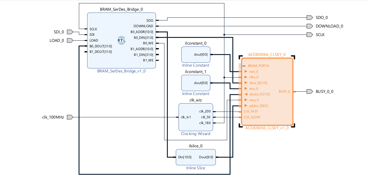
The core is fully controlled through read/write operations on a BRAM (optionally accessible via an AXI BRAM_CONTROLLER). The instantiated BRAM is 1 True Dual Port with port A available to the user and port B managed by the internal Math Engine. The BRAM has a width of 32 bits and a depth of 1024 locations. The core uses the first 67 locations (0–66), with the remaining ones completely available for the user via port A.
| ID | ADDRESS | VARIABLE | DIR | FORMAT | Note |
|---|---|---|---|---|---|
| BRAM_0 | 0 | START_CMD | IN-OUT | BINARY | Set to 0x1 by the user to start the computation. Set to 0x0 by the math engine at the end of computation. |
| BRAM_0 | 1 | DNA1 | OUT | BINARY | FPGA DNA (MSB) populated after initialization. |
| BRAM_0 | 2 | DNA2 | OUT | BINARY | FPGA DNA (LSB) populated after initialization. |
| BRAM_0 | 3 | USER_KEY1 | IN | BINARY | LICENSE_KEY (MSB) input required for validation. |
| BRAM_0 | 4 | USER_KEY2 | IN | BINARY | LICENSE_KEY (LSB) input required for validation. |
| BRAM_0 | 5 .. 25 | H00 .. H55 | IN | FLOAT32 | Symmetric matrix lower-triangular elements ($H_{00}, H_{10}, H_{11}, \dots, H_{55}$, 21 elements total). |
| BRAM_0 | 26 .. 31 | b0 .. b5 | IN | FLOAT32 | Right-hand side vector elements ($b_0$ through $b_5$). |
| BRAM_0 | 32 .. 37 | dx0 .. dx5 | OUT | FLOAT32 | Output correction vector result elements ($\Delta x_0$ through $\Delta x_5$). |
| BRAM_0 | 38 .. 58 | L00 .. L55 | OUT | FLOAT32 | Cholesky lower-triangular factor elements ($L_{00}, L_{10}, L_{11}, \dots, L_{55}$, 21 elements total). |
| BRAM_0 | 59 .. 64 | y0 .. y5 | OUT | FLOAT32 | Forward substitution intermediate vector elements ($y_0$ through $y_5$). |
| BRAM_0 | 65 .. 66 | RESERVED | N/A | RESERVED | Internal engine scratchpad registers. |
In addition to the BRAM interface, the core exposes:
CLK_SLOW is used for the initialization and for access to the DNA reader primitive ($50\text{ MHz}$)CLK_FAST is used to drive the internal computation engine (Max Frequency: $200\text{ MHz}$)BUSY pin that, when set to high, signals when the core is executing the initialization or its main function.
The core, at power-up, performs an initialization sequence that lasts (with CLK_SLOW @ $50\text{ MHz}$) less than $5,000\text{ ns}$, populating the BRAM with the DNA of the FPGA. Once initialized, the user loads the BRAM inputs and sets START_CMD to 0x1. Results are written in BRAM after exactly 1,268 clock cycles ($6.34\ \mu\text{s}$ @ $200\text{ MHz}$), and the core clears START_CMD to 0x0 and sets BUSY=0.
Note: if the USER_KEY is not correct, the core terminates in the specified timeframe, but produces unpredictable results.
To validate the numerical integrity and dynamic range stability of the ACE808066 computing fabric, the hardware engine was subjected to a rigorous, 30-stage hardware-in-the-loop simulation test sweep. The verification manifest intentionally sweeps the input symmetric matrix ($H$) and the right-hand-side vector ($b$) across multiple orders of magnitude, forcing the internal single-precision floating-point (float32) pipelines to calculate variations spanning from macro-scale values ($\sim 10^4$) down to sub-fractional micro-signals ($\sim 10^{-8}$).
As compiled in the hardware validation report below, the core achieved 100% numerical equivalence with zero precision breaches across all evaluated operating envelopes. Peak relative deviation was bounded at 0.00251% under sub-fractional stress loading (Stage 24), while nominal tracking bounds routinely converged to 0.00000% error, demonstrating true IEEE-754 bit-perfect math propagation.
=======================================================================================
         ACE808066 CHOLESKY SOLVER ENGINE: ACCURACY REPORT
=======================================================================================
--- Evaluation Stage 1 (Macro-Scale ~10^4) ---
Element |   Golden Float   |   Actual HW Float   |   Abs Error   | Relative Err % | Status
---------------------------------------------------------------------------------------
  dx0   |    -1.1237e+04   |       -1.1237e+04   |    9.77e-04   |        0.00001%  |  PASS
  dx1   |     9.3660e+03   |        9.3660e+03   |    0.00e+00   |        0.00000%  |  PASS
  dx2   |     1.0122e+04   |        1.0122e+04   |    9.77e-04   |        0.00001%  |  PASS
  dx3   |    -2.2240e+03   |       -2.2240e+03   |    2.44e-04   |        0.00001%  |  PASS
  dx4   |    -1.5283e+04   |       -1.5283e+04   |    9.77e-04   |        0.00001%  |  PASS
  dx5   |     3.0617e+03   |        3.0617e+03   |    0.00e+00   |        0.00000%  |  PASS
Result:  STAGE 1 VERIFICATION SUCCESSFUL

--- Evaluation Stage 5 (Micro-Signals ~10^-8) ---
Element |   Golden Float   |   Actual HW Float   |   Abs Error   | Relative Err % | Status
---------------------------------------------------------------------------------------
  dx0   |    -3.9262e-08   |       -3.9262e-08   |    3.55e-15   |        0.00001%  |  PASS
  dx1   |     3.4090e-07   |        3.4090e-07   |    2.84e-14   |        0.00001%  |  PASS
  dx2   |     3.8861e-07   |        3.8861e-07   |    2.84e-14   |        0.00001%  |  PASS
  dx3   |     9.6240e-09   |        9.6240e-09   |    8.88e-16   |        0.00001%  |  PASS
  dx4   |    -3.8390e-08   |       -3.8390e-08   |    3.55e-15   |        0.00001%  |  PASS
  dx5   |     8.4484e-08   |        8.4484e-08   |    2.13e-14   |        0.00003%  |  PASS
Result:  STAGE 5 VERIFICATION SUCCESSFUL

--- Evaluation Stage 24 (Peak Relative Deviation Stress Stage) ---
Element |   Golden Float   |   Actual HW Float   |   Abs Error   | Relative Err % | Status
---------------------------------------------------------------------------------------
  dx0   |     9.2261e-05   |        9.2261e-05   |    2.18e-11   |        0.00002%  |  PASS
  dx1   |     7.7369e-07   |        7.7368e-07   |    1.94e-11   |        0.00251%  |  PASS
  dx2   |    -3.2994e-04   |       -3.2994e-04   |    0.00e+00   |        0.00000%  |  PASS
  dx3   |     3.7307e-05   |        3.7307e-05   |    1.46e-11   |        0.00004%  |  PASS
  dx4   |     3.6785e-04   |        3.6785e-04   |    5.82e-11   |        0.00002%  |  PASS
  dx5   |    -3.3024e-04   |       -3.3024e-04   |    2.91e-11   |        0.00001%  |  PASS
Result:  STAGE 24 VERIFICATION SUCCESSFUL

--- Evaluation Stage 30 ---
Element |   Golden Float   |   Actual HW Float   |   Abs Error   | Relative Err % | Status
---------------------------------------------------------------------------------------
  dx0   |    -1.1534e-07   |       -1.1534e-07   |    2.13e-14   |        0.00002%  |  PASS
  dx1   |    -1.3123e-07   |       -1.3123e-07   |    2.84e-14   |        0.00002%  |  PASS
  dx2   |    -7.1549e-08   |       -7.1549e-08   |    1.42e-14   |        0.00002%  |  PASS
  dx3   |     2.7729e-07   |        2.7729e-07   |    0.00e+00   |        0.00000%  |  PASS
  dx4   |     8.1359e-08   |        8.1359e-08   |    7.11e-15   |        0.00001%  |  PASS
  dx5   |    -2.8226e-08   |       -2.8227e-08   |    8.88e-15   |        0.00003%  |  PASS
Result:  STAGE 30 VERIFICATION SUCCESSFUL
=======================================================================================
 FINAL REPORT: SUCCESS (All 30 stages match within 0.01% error limit)
=======================================================================================ACE808066 is delivered as a pre‑packaged Vivado IP core, ready for integration through the AMD/Xilinx IP Catalog. Each licensed core includes:
USER_KEY file for license activation
ACE provides a USER_KEY value (64 bits) for FPGA Serial Number (DNA for AMD/Xilinx). The keys are delivered in a simple CSV file:
DNA_HEX,AUTHORIZATION_KEY
0011223344556677,C303E222F7D44C5B
ABCDE1234567890F,A2A3A3114194ED74
5566778899AABBCC,94C023F594AA6F63
DEADBEEF12345678,F40237F85DFB6F2A
00123456789ABCDE,E8ACBBDBFCF3ACB7
...............,.................BRAM_PORTA interface (addresses 1 and 2).USER_KEY corresponding to the FPGA SN in the ACE provided USER_KEY file.USER_KEY via the BRAM_PORTA interface (addresses 3 and 4).
The keys are generated on customer order. In simulation, a demo DNA is used and the corresponding USER_KEY is provided in the file for a seamless experience.
Pricing is provided directly by ACE based on deployment volume, license type, optional customization requirements, and target FPGA family.
Data Privacy note: By contacting us via email, you agree that we will use your provided contact details and mathematical specifications solely to evaluate project feasibility during our early-access phase. We do not sell or share your personal information with third parties. We may use standard web analytics tools to monitor basic, aggregated website traffic to improve our site performance.